Micro-Patterned Filters

Our micro-patterned optical filters combine patented microlithography expertise with state-of-the-art coating technology to enable smaller and simpler optical designs for portable or complex optical systems. This exclusive technology allows patterning multiple dielectric, metal, and color filter arrays on a single substrate.
Standardized processes have been developed and are used today to manufacture these filter arrays in a new, world-class optical semiconductor waferfab designed explicitly for this purpose. The process is scalable to wafer-level glass or semiconductor volume production and supports millions of custom micro-patterned optical devices delivered annually.
Salvo Coatings patterned coatings are used to enhance performance in many biomedical, industrial, and aerospace OEM applications – enabling next-generation integrated optical devices that are more compact, robust, and cost-effective.
Here at Salvo Technologies focus our operations on supporting customers in developing their next-generation imaging and sensing equipment. With a toolbox of processes and technologies, we can quickly design the most effective way to develop products based on your application or product functionality. Our application engineers work with you to quickly assess your requirements and provide a proposal of technical feasibility.
Some of the design parameters and decisions are based on the following:
- Substrate: semiconductor wafers, optical-grade glass, fused silica, or other materials
- Number of filter bands combined on one substrate (multispectral sensing)
- Filter design parameters: transmission bands, blocking specifications
- Feature geometries: smallest size, tolerance in position
- Alignment accuracies and available alignment markers
- Defined (e.g., ESD) handling, dicing, finishing, testing, and packaging
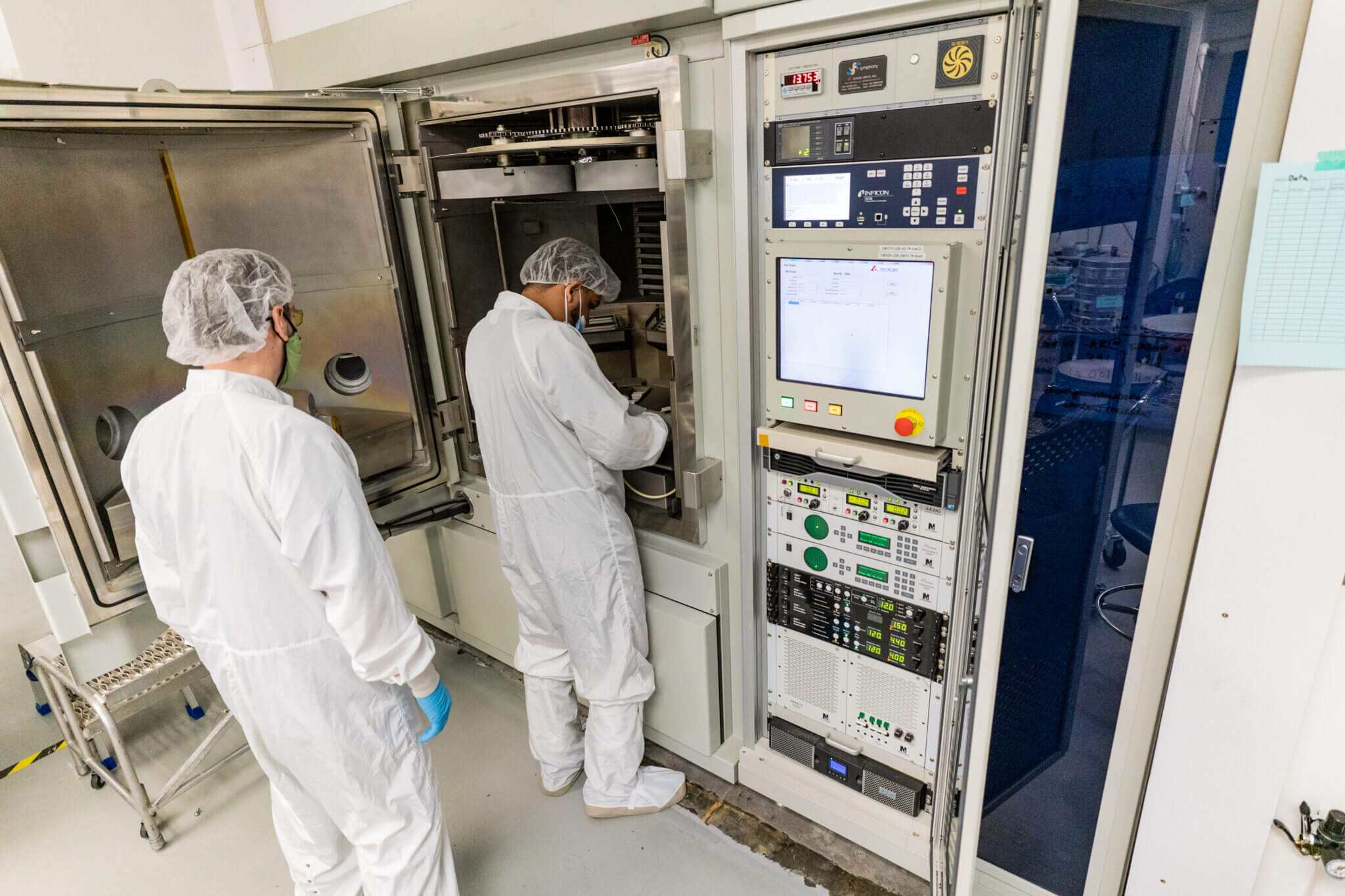
The equipment in our Class 100/1000 wafer fabrication cleanrooms have been selected and custom-designed for micro-patterned coatings, enabling us to support ultra-small (μm) pixel-level features for imaging applications. We use the latest coating technology, including IAD evaporation, magnetron sputtering, and ion beam sputtering techniques.
Semiconductor-style mask aligners handle wafers up to 8 inches in the lithography fab.
Currently, we can implement and combine the following designs and materials:
- Custom wavelength bands | UV, VIS, NIR, SWIR
- Dichroic | bandpass, short-wave pass, long-wave pass, BBAR & more
- Metallic | high reflector, dark absorber, apertures, neutral density & more
Optical Technology
- Multispectral sensing for spectroscopy
- Multispectral imaging with custom CCD & CMOS sensors
- Precision reticles & alignment patterns
- Patterned pixels & apertures
- Focal plane arrays (FPA)
- Color mixing & dimming
- Variable/gradient filters
Patents cover our patterned optical filters in micro-patterning technologies (US patent 7648808) and pixel filter array on substrate (either on glass or directly on sensor/detector wafers) methodologies (US patent 6638668).
- Non-invasive biomedical imaging
- Remote sensing for satellites, defense & precision agriculture
- Industrial quality control sensing & imaging
- Color mixing for entertainment lighting
- Light intensity control in industrial equipment
- Sensing for consumer wearables
- Integrated custom optics for scientific devices
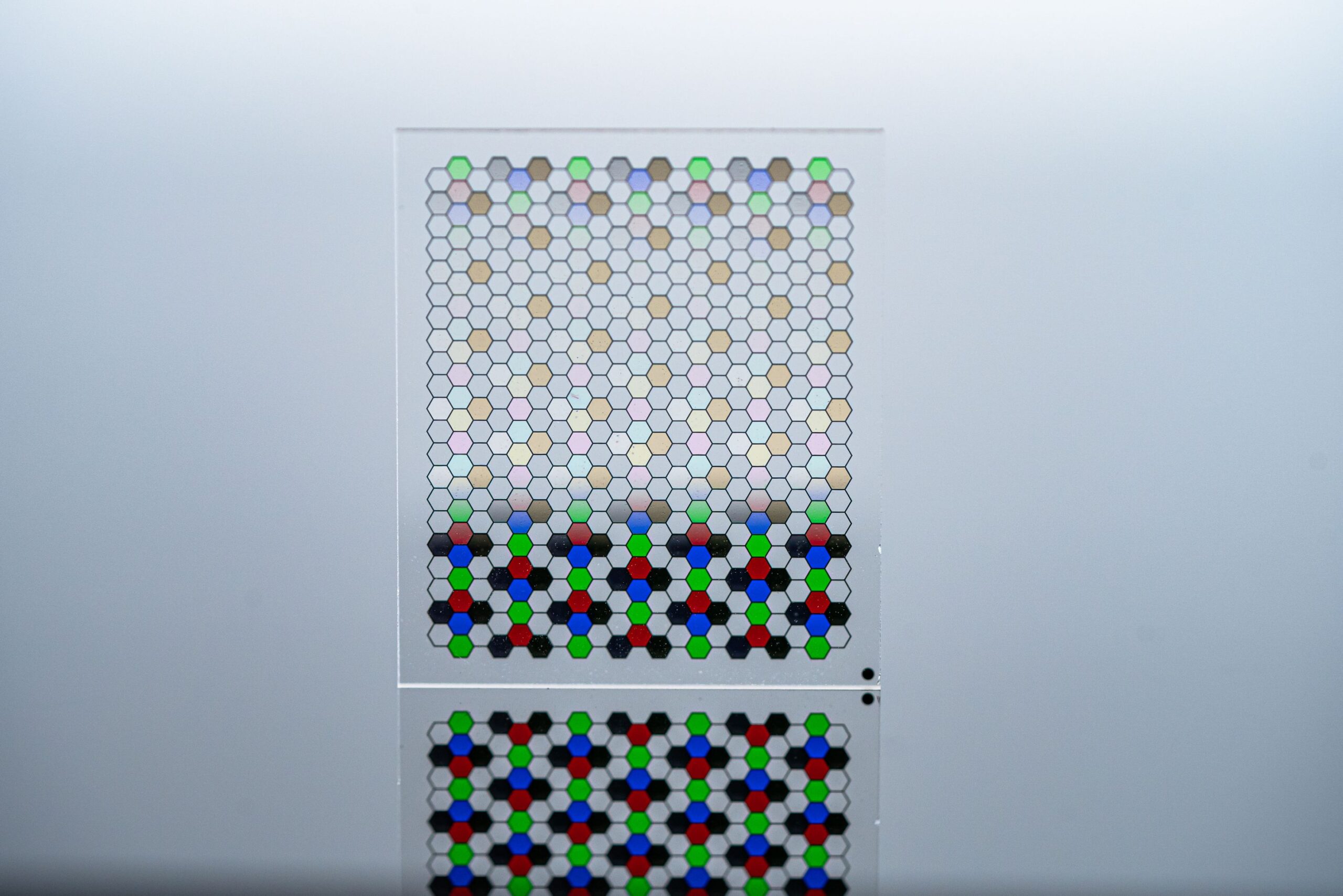
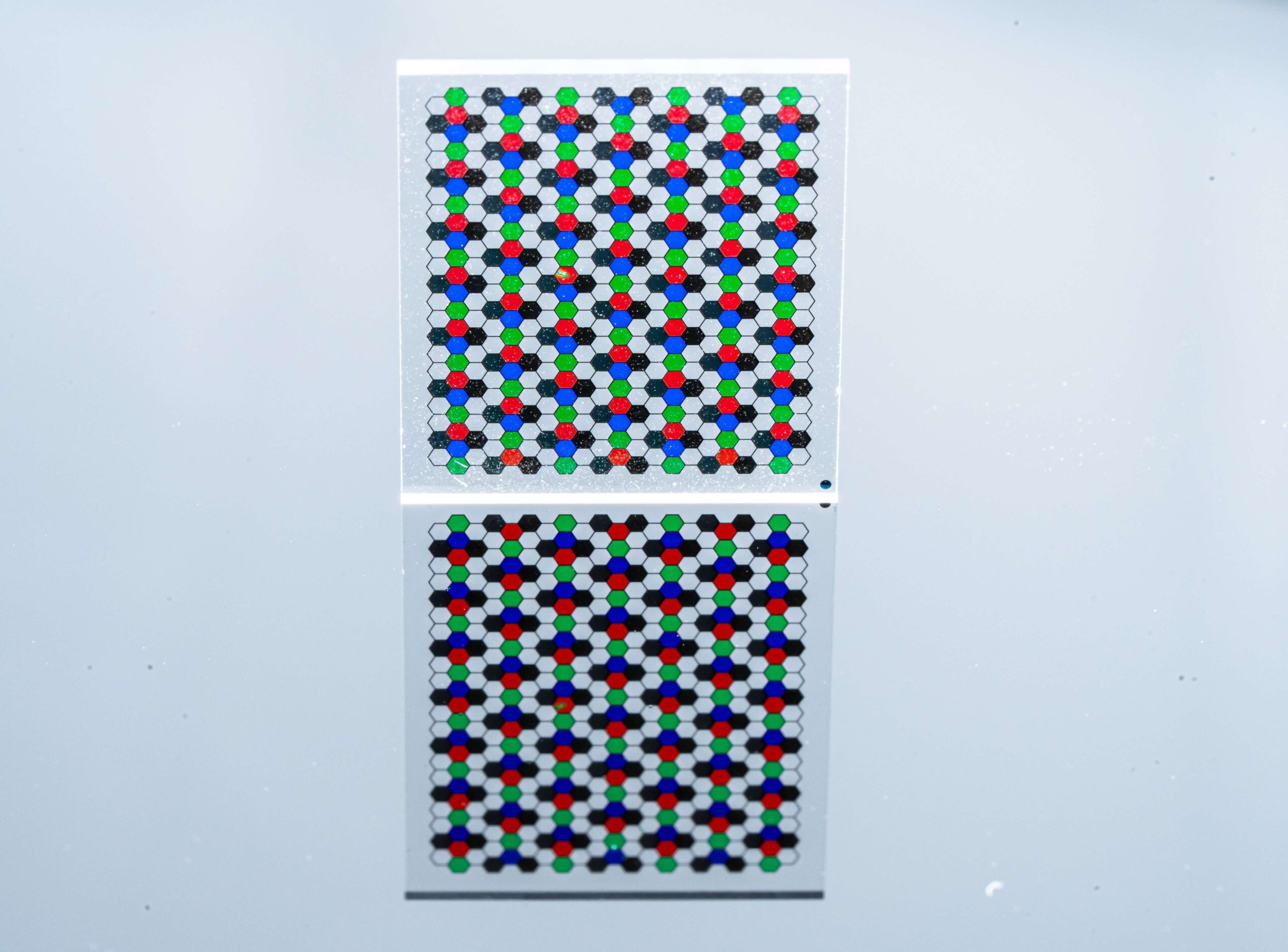
Bayer Filters
- Custom Bayer & mosaic filters created with standard RGB gels, dichroic coatings, or a combination
- Simultaneous acquisition of all wavelengths allows for point & shoot, and real-time data
- Reduces SWaP, allowing for applications with minimal space (UAV)
Active Wafer Deposition
- High volume for semiconductor & cell phone industries
- Processing of customer-supplied material (up to 8 inches)
- Improved S/N on ambient light, proximity & biometric sensors
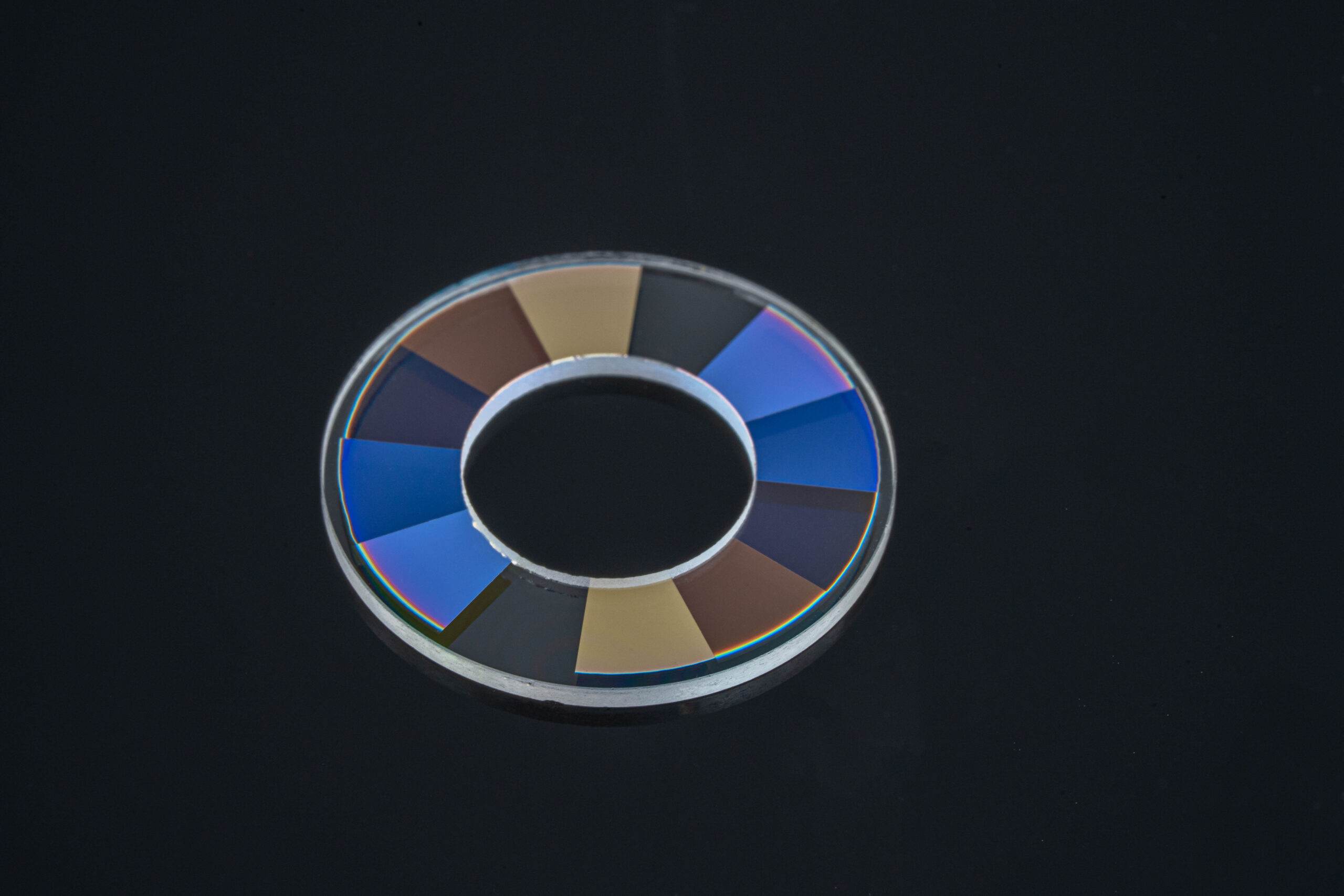
Mosaic Filters
High-performance Pattern Dicrohic filter.
- Space-qualified filters used for multispectral imaging
- Narrow line widths & minimal unusable space between filters
- Options from VIS to SWIR ranges
- Allow customers to have multiple bandpass filters on one substrate for one camera, eliminating the need for multiple cameras in one system.
- Custom patterned filters with up to 9 bands on one substrate. We can pattern on glass or semiconductor wafers.
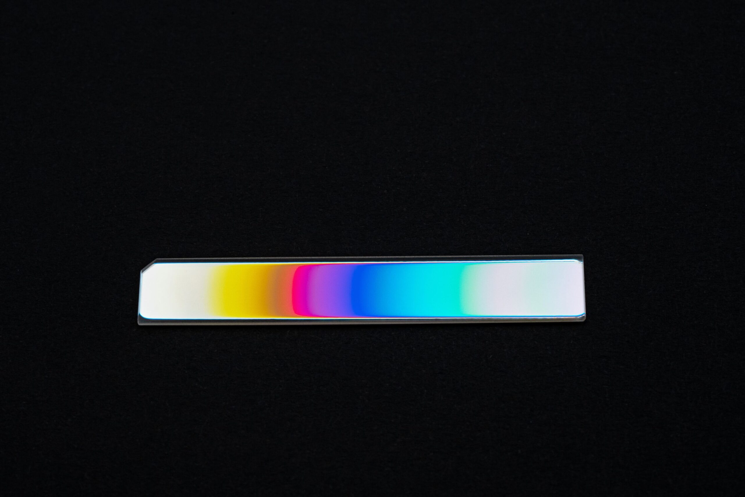
Linear Variable Filters & LVBPF
- Varies in blocking reflection in a predictable and linear pattern across an optic.
- Used for Sensing & Hyperspectral Imaging
- Gives hundreds of distinct filters on one substrate.
Stripe Filters
- Space-qualified filters used for multispectral imaging
- Narrow line widths & minimal unusable space between filters
- Options from VIS to SWIR ranges
- Custom patterned filters with up to 9 bands on one substrate. We can pattern on glass or semiconductor wafers.
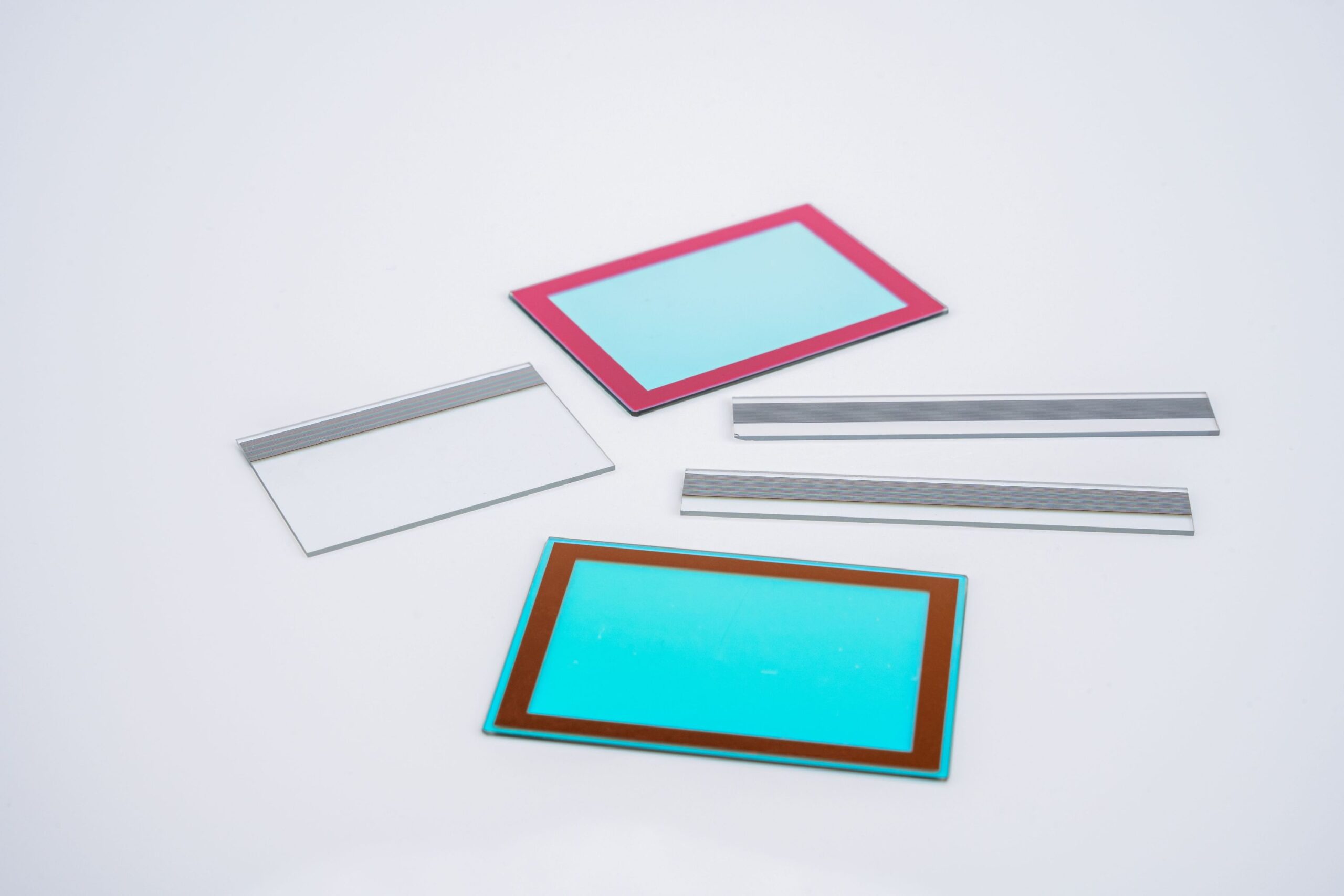
Butcher Block Filters
- Multiple high-performance dichroic coatings bonded together side by side.
- Used for large features sized sensing (+1mm)
- Allows customers to work with one filter rather than multiple substrates.
Gradient Filters
- Fine quasi-stochastic pattern
- Smooth fades & mixing
- Dimming